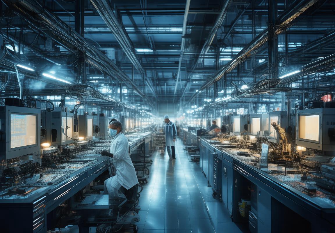
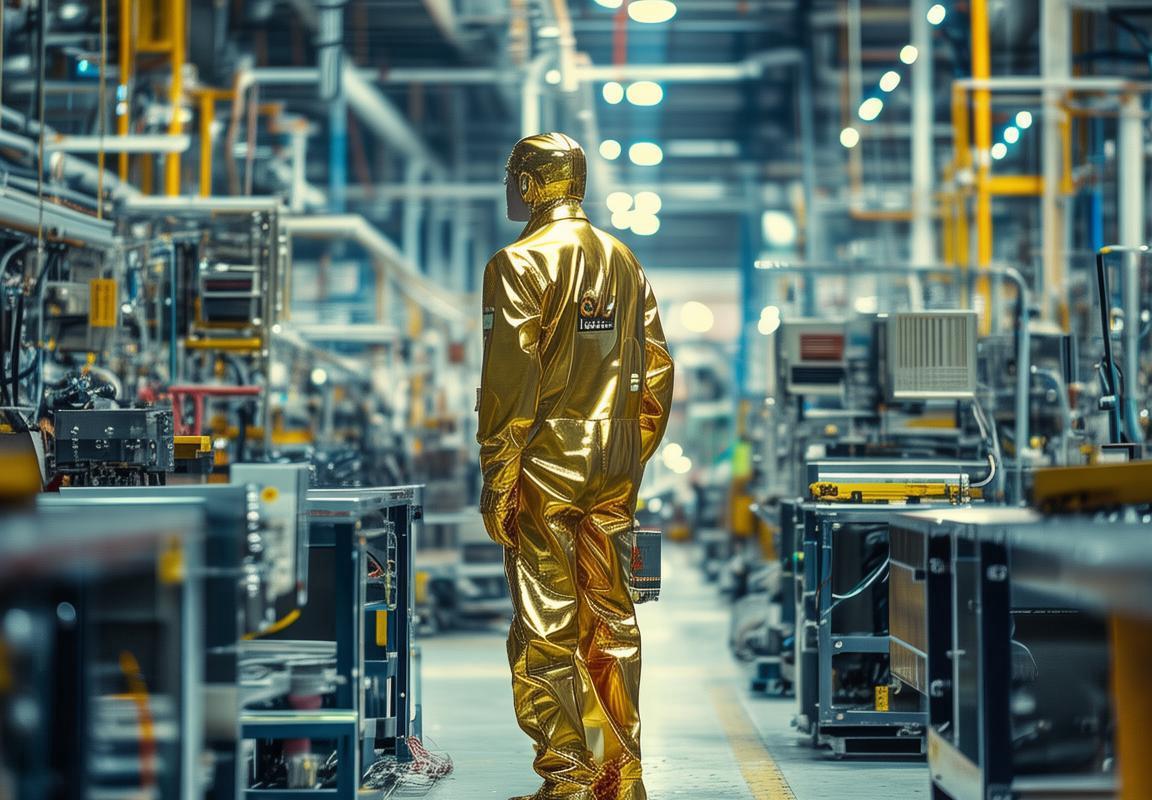
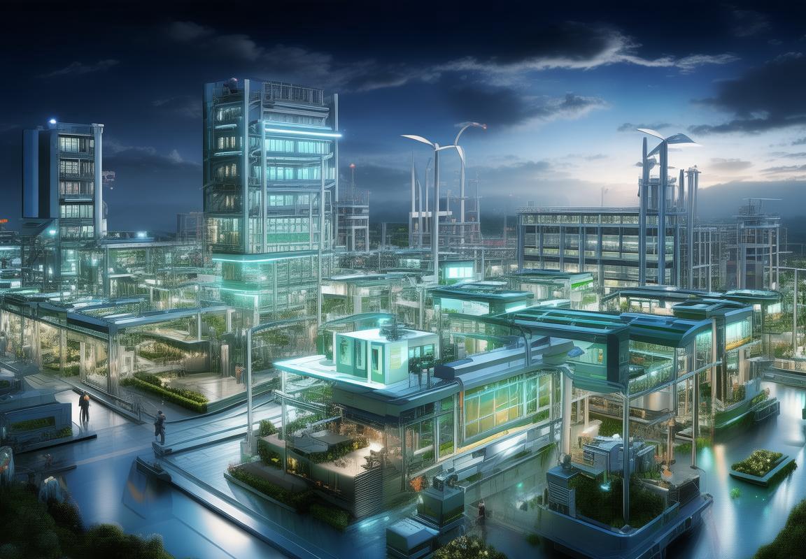
In the intricate tapestry of modern technology, the integrated circuit board (ICB) factory stands as a cornerstone of innovation. These facilities are not just assembly lines; they are hubs of creativity and precision, where the future is shaped with each new chip that rolls off the line. Today, we delve into the role these factories play in driving future tech developments, highlighting the impact they have on our world and the path they are paving for the next generation of technological marvels.
The Heart of Innovation Exploring the Integrated Circuit Board Factory
Nestled at the forefront of technological marvels, the integrated circuit board (ICB) factory stands as the beating heart of innovation. These bustling hubs of precision and precision are where the digital world is crafted, where the smallest components come together to create the largest impacts. Let’s take a journey into the intricate world of ICB factories, where creativity meets cutting-edge engineering.
In the heart of these factories, you’ll find a symphony of activity, a dance of machines and hands that bring to life the intricate designs of tomorrow. The walls are lined with rows of equipment, each a precision instrument in the grand orchestra of electronics manufacturing. Here, the process begins with the most basic of elements: silicon wafers, mere slivers of pure silicon that will eventually become the foundation for countless circuits.
The journey of an ICB starts with the design phase, where engineers sketch out the blueprint of the circuit board. These blueprints are then translated into a digital format, ready for the next step. The wafer, a thin disk of silicon, is the canvas upon which the future circuits will be drawn. It’s a meticulous process, one that requires a balance of art and science, as engineers carefully etch patterns into the silicon, creating the pathways that will allow electricity to flow.
Once the patterns are etched, the wafer is sent through a series of chemical baths and thermal treatments. These steps are crucial, as they prepare the wafer for the next layer of complexity. The layers of copper are then deposited onto the wafer, creating the conductive pathways that will connect the various components of the circuit.
The next phase is the assembly of the components. Tiny resistors, capacitors, and transistors are placed onto the copper pathways with a level of precision that would make a watchmaker’s hand tremble. This is done using automated pick-and-place machines, which can place hundreds of components in a matter of seconds. The components are then bonded to the copper with a heat-sensitive adhesive, creating a permanent connection.
After the components are in place, the board undergoes a series of tests to ensure that each connection is sound and that the circuit operates as intended. These tests are not just about quality control; they are about ensuring that the board can withstand the rigors of real-world use. The boards are subjected to temperature extremes, electrical stress, and mechanical shock, all to prove their durability.
The technology within ICB factories is a marvel in itself. Advanced etching techniques, like photolithography, allow for the creation of circuits with features as small as a few nanometers. The equipment used is sophisticated, requiring a skilled workforce to operate it. Robots and automated systems work alongside human engineers, each contributing to the seamless production of these complex circuits.
As the ICBs move through the factory, they are constantly monitored and inspected. The quality control process is rigorous, with each board being checked at multiple stages to ensure that it meets the exacting standards of the electronics industry. This attention to detail is what separates a good ICB from a great one.
But the impact of ICB factories extends beyond the walls of the factory floor. These facilities are the backbone of the global supply chain, providing the essential components for everything from smartphones to spacecraft. The efficiency and scale of ICB production have a direct effect on the cost and availability of technology worldwide.
Innovation is the lifeblood of ICB factories. New materials, such as gallium nitride, are being explored to improve the efficiency of power electronics. Researchers are also looking into new ways to integrate sensors and actuators directly onto the circuit board, creating what are known as “system-in-package” solutions. These advancements are not just about making better circuits; they are about making entire systems more efficient and compact.
The environmental considerations of ICB factories are also a growing concern. As the demand for electronics continues to rise, so does the need to be sustainable. Factories are investing in energy-efficient equipment and recycling programs to minimize their environmental impact. The goal is to create a more sustainable and eco-friendly manufacturing process without compromising on quality.
In the end, the ICB factory is a testament to human ingenuity and the relentless pursuit of progress. It’s a place where the impossible becomes possible, where the future is being built one circuit at a time. As we continue to push the boundaries of technology, the role of the ICB factory will only grow more critical, ensuring that our world remains connected, efficient, and innovative.
The Essence of an Integrated Circuit Board (ICB
Integrated circuit boards, often abbreviated as PCBs, are the unsung heroes of the modern technological world. These intricate pieces of technology are the backbone of almost every electronic device we use daily. To understand the essence of an ICB, one must delve into its design, function, and the myriad of innovations that have shaped its evolution.
The foundation of an ICB lies in its ability to integrate thousands, even millions, of electronic components onto a single, flat board. This miniaturization is no small feat, as it allows for devices to become smaller, more powerful, and more efficient. At the heart of an ICB is the semiconductor material, typically silicon, which acts as the canvas for the electronic circuitry.
The process of creating an ICB starts with the layout of the circuitry, which is meticulously designed to ensure that each component is placed precisely where it needs to be. This design is crucial for the functionality and performance of the device, as the connections between components must be optimized for speed and reliability.
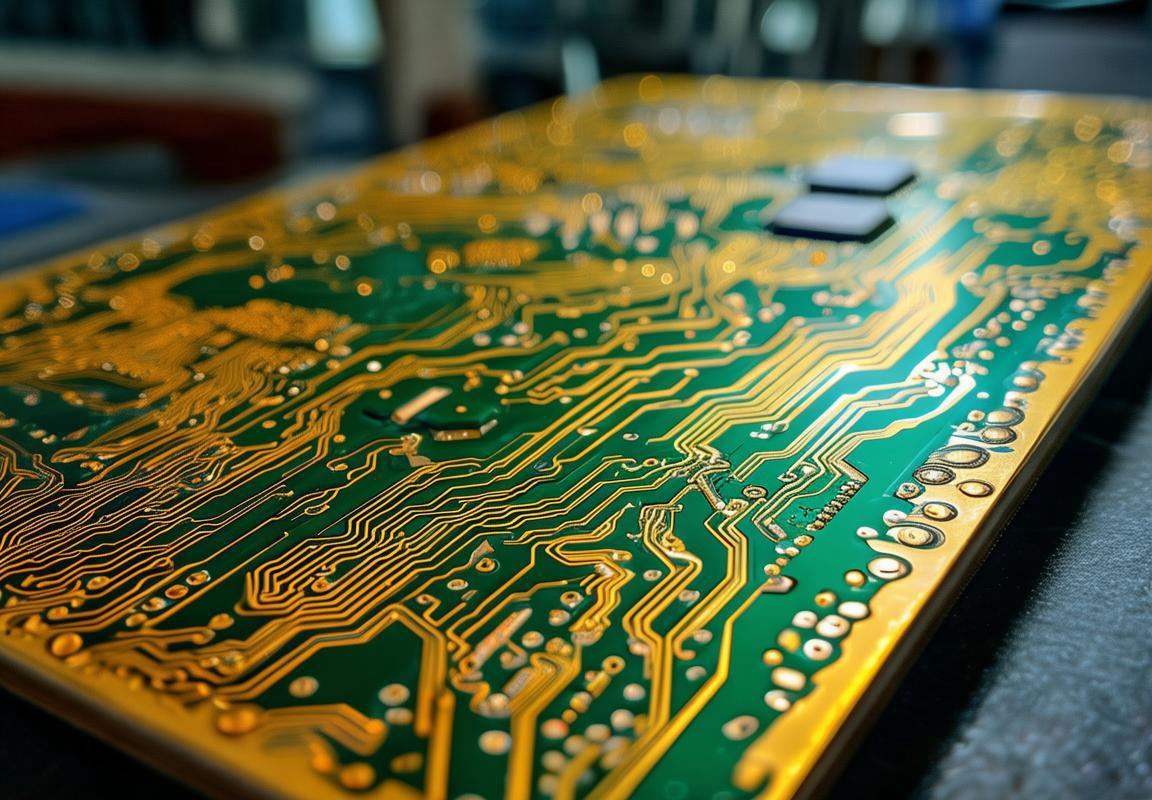
Once the layout is finalized, the board moves through a series of manufacturing steps. The first step is the creation of a substrate, which is usually a glass-like material called fiberglass. This substrate is then coated with a layer of copper, which will eventually form the pathways for the electrical signals.
The copper layer is then etched to define the precise paths for the electrical connections, creating a network of tracks that interconnect the various components. These tracks are incredibly thin, often measured in micrometers, and must be highly accurate to ensure the board’s reliability.
After the copper tracks are etched, they are insulated with a layer of solder mask, which prevents electrical shorts and protects the copper from environmental damage. This mask is typically green, hence the common term “green PCB,” but it can come in various colors.
Next comes the drilling of holes through the substrate and the copper layers. These holes, known as via holes, allow for the connection of the copper tracks on different layers of the board. The drilling process must be precise, as any misalignment can lead to a faulty board.
The final layers of the ICB are the components themselves. These can range from simple resistors and capacitors to complex integrated circuits that contain thousands of transistors. The components are soldered onto the board using a process called surface mount technology (SMT), which is highly automated and allows for a dense packing of components.
The essence of an ICB is not just in its manufacturing process, but in its versatility. ICBs come in various sizes, shapes, and complexities, from the tiny PCBs in a smartphone to the large, complex boards in a data center. Each board is tailored to the specific needs of the device it will power, whether it’s a medical device, a gaming console, or an automotive system.
The performance of an ICB is determined by several factors. The quality of the materials used, such as the copper and the fiberglass, is critical. The precision of the manufacturing process, particularly the etching and drilling, must be within tight tolerances to ensure that the electrical signals flow smoothly. The design of the circuitry itself must be optimized for the intended application, balancing power, speed, and efficiency.
Moreover, the reliability of an ICB is paramount. Devices are often subjected to harsh conditions, including temperature extremes, vibration, and moisture, and the PCB must withstand these to function properly over its lifetime. This reliability is achieved through rigorous testing and quality control throughout the manufacturing process.
Innovation in the field of ICBs is constant. New materials, such as high-frequency laminates, are being developed to support the ever-increasing demands of high-speed data transfer. Advanced manufacturing techniques, like 3D PCBs, allow for even more complex and compact designs. The ability to integrate more components onto a single board continues to push the boundaries of what is possible in electronics.
The essence of an ICB is a testament to human ingenuity and the relentless pursuit of progress. It’s a marvel of modern engineering, a platform that enables the countless innovations that have transformed our lives. From the smallest microcontroller to the most powerful supercomputer, the ICB is the silent partner that makes it all possible.
The Significance of an ICB Factory
An ICB factory stands as a cornerstone in the modern technological landscape, embodying a fusion of precision engineering, cutting-edge manufacturing, and relentless innovation. These factories are not merely production hubs; they are the beating hearts of the electronics industry, where the dreams of tomorrow are crafted into tangible realities.
In these bustling facilities, a symphony of intricate processes unfolds, each step contributing to the creation of the essential building blocks of our digital world. The significance of an ICB factory is multifaceted, encompassing its role in economic growth, technological advancements, and the societal impact it has on our daily lives.
The economic impact is profound. ICB factories are job creators on a massive scale, offering employment opportunities across various skill levels. From engineers and technicians to assembly line workers and quality control inspectors, these factories require a diverse workforce. The ripple effect of this economic activity is felt far beyond the factory gates, supporting local communities and contributing to the national GDP.
Technologically, ICB factories are at the forefront of innovation. They are the birthplace of new designs, manufacturing techniques, and materials that push the boundaries of what’s possible. The relentless pursuit of miniaturization, efficiency, and power has led to the development of smaller, faster, and more energy-efficient chips. These advancements don’t just benefit the electronics industry; they spill over into other sectors, from healthcare to transportation, where smaller, more efficient devices are in high demand.
Innovation is not just about creating new products; it’s also about solving complex problems. ICB factories are at the center of this intellectual endeavor, turning challenges into opportunities. For instance, the development of new chip architectures has enabled advancements in artificial intelligence, allowing machines to learn, reason, and make decisions more effectively. This has profound implications for industries ranging from data analysis to autonomous vehicles.
The societal impact of ICB factories is undeniable. The devices we rely on daily—our smartphones, computers, and medical equipment—all owe their existence to these factories. The speed at which we communicate, the quality of healthcare we receive, and the efficiency of our transportation systems are all influenced by the chips that these factories produce. The integration of technology into our lives has been made possible by the relentless work and dedication of the professionals who work within these factories.
The global reach of ICB factories is extensive. They are not just local businesses; they are global players in a highly interconnected market. The export of chips and related technologies is a significant revenue stream for many countries. This global trade fosters international collaboration and strengthens diplomatic ties, as countries depend on one another for the latest innovations.
Furthermore, the supply chain of ICB factories is complex and interdependent. These factories require raw materials from all over the world, and the products they manufacture are often components of larger, more complex systems. This interconnectedness means that disruptions in one part of the supply chain can have cascading effects across the entire industry.
In the realm of sustainability, ICB factories face unique challenges. The production of chips is energy-intensive and requires careful management of hazardous materials. However, these factories are also at the forefront of developing environmentally friendly practices. From the recycling of materials to the reduction of waste and energy consumption, these factories are increasingly mindful of their ecological footprint.
As we look to the future, the significance of ICB factories is only expected to grow. The demand for advanced chips is skyrocketing, driven by the rise of the Internet of Things (IoT), 5G networks, and the ongoing digital transformation of industries. The factories that can adapt to these changing demands will be the ones that lead the way in the next wave of technological advancements.
In conclusion, ICB factories are not just places where circuits are etched onto silicon wafers. They are hubs of creativity, efficiency, and economic power. They shape our world in ways we often take for granted, and their importance in the global landscape is as undeniable as the technologies they produce. As we continue to rely on the innovations that emerge from these factories, their role in our lives is sure to remain indispensable.
The Manufacturing Process Unveiled
The intricate dance of technology unfolds within the walls of an integrated circuit board (ICB) factory, where the manufacturing process is a symphony of precision and innovation. From the initial design to the final product, each step is crucial in crafting the heart of modern electronics.
In the heart of the factory, engineers and technicians work tirelessly to transform raw materials into the complex web of circuits that will power tomorrow’s devices. The journey begins with a blueprint, a digital design that outlines the intricate pattern of the circuits that will be etched onto the silicon wafer.
The wafer itself is a marvel of engineering, a thin slice of pure silicon, the bedrock of the electronic world. It’s polished to a mirror finish and treated with chemicals to create a surface that will accept the delicate layers of metal and insulating materials. This process, known as wafer preparation, is meticulous, as any imperfection can lead to a faulty chip.
Once the wafer is prepped, the next step is photolithography. Here, a mask, or a patterned transparency, is placed over the wafer. A light-sensitive chemical, or photoresist, is then applied to the surface. When exposed to ultraviolet light through the mask, the photoresist hardens in the areas that align with the circuit pattern. The unexposed areas are washed away, leaving a negative image of the circuit design on the wafer.
The wafer is then baked to remove any remaining photoresist and to harden the exposed areas, which serve as a guide for the next steps. This is followed by etching, a chemical process that removes the unwanted silicon around the exposed circuit patterns. The result is a raised pattern on the wafer, which is then coated with a thin layer of metal, typically copper, through a process called electroplating.
The metal layer is then etched to match the circuit pattern, leaving tiny copper lines that will connect the transistors and other components on the wafer. This is where the complexity of the ICB really takes shape, as the patterned metal lines form the pathways that allow electrical signals to flow through the chip.
After the metal lines are in place, the wafer is treated with an insulating material, usually silicon dioxide, to prevent short circuits. This layer is then etched to create the necessary gaps and vias, which are pathways that connect the layers of the chip vertically.
The wafer is now ready for the addition of the transistors and other components. This is done through a process called doping, where impurities are introduced into the silicon to alter its electrical properties. The doping creates regions of the silicon that act as sources, drains, and gates for the transistors.
The wafer is then coated with a layer of insulation, and another layer of metal is applied. This process is repeated multiple times, with each layer adding more complexity to the chip. Each layer is etched to create the necessary connections, and the process is repeated until the desired level of integration is achieved.
Once the wafer is fully processed, it’s time for testing. Each chip is tested individually to ensure it meets the required specifications. This is a critical step, as any defects in the manufacturing process can lead to a faulty chip.
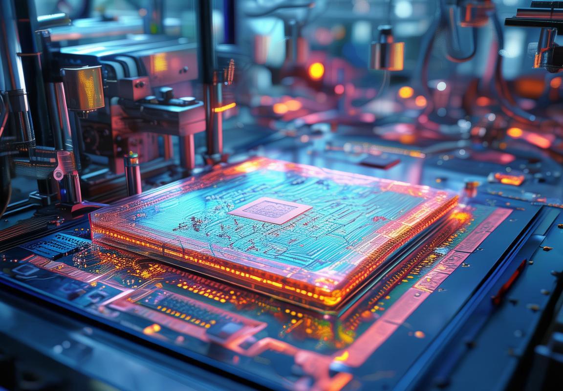
The final step in the manufacturing process is packaging. The individual chips are mounted onto a substrate, which is then encapsulated in a protective material. This packaging not only protects the chip but also provides the electrical connections needed to connect the chip to the outside world.
Throughout the entire process, the ICB factory relies on a combination of human expertise and cutting-edge automation. The precision required to manufacture a single chip is mind-boggling, with each step requiring a high degree of accuracy and control. The result is a product that is not just a piece of silicon, but a testament to human ingenuity and the relentless pursuit of technological advancement.
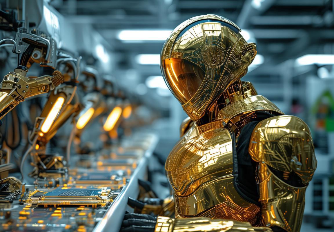
State-of-the-Art Technology in ICB Production
In the world of integrated circuit (IC) production, staying ahead of the curve is paramount. Factories that manufacture these critical components for a wide range of electronic devices rely on cutting-edge technology to ensure precision, efficiency, and reliability. Here’s a glimpse into the state-of-the-art technology shaping ICB production.
Precision in every layerManufacturing an ICB involves creating layers upon layers of intricate circuits on a tiny silicon wafer. To achieve this, factories employ advanced photolithography techniques. These methods use light to project a pattern onto a silicon wafer, which is then etched into the wafer’s surface with extreme precision. The latest machines can create patterns with features as small as 10 nanometers, a fraction of the width of a human hair.
Automated processesAutomation is key to maintaining the high standards required for ICB production. Factories deploy automated systems that can handle tasks like wafer handling, cleaning, and inspection. These robots are programmed to work in harmony, ensuring that each wafer is processed without human error. From loading to unloading, every step is streamlined, reducing the likelihood of defects and improving overall yield.
Advanced etching techniquesEtching is a crucial process that removes unwanted material from the wafer’s surface. Modern ICB factories use advanced etching technologies that are capable of selectively removing materials with nanoscale accuracy. These techniques, such as reactive ion etching (RIE) and chemical mechanical planarization (CMP), help to create the necessary channels and vias for the electronic components.
High-k dielectricsTo improve the performance of ICBs, manufacturers are increasingly using high-k dielectrics, which have a higher dielectric constant than traditional silicon dioxide. These materials can reduce the leakage current in transistors, leading to lower power consumption and faster switching speeds. The ability to fabricate these high-k dielectrics at the nanoscale is a testament to the advanced technology in ICB production.
Three-dimensional (3D) ICsThe demand for more powerful and efficient chips has driven the development of 3D ICs. These chips stack multiple layers of transistors vertically, which can significantly increase the density of the integrated circuits. The production of 3D ICs requires specialized equipment that can bond different layers together and then etch the necessary connections. Precision and alignment are paramount in this process.
High-speed wafer probingTo test the functionality of ICBs before they are packaged, high-speed wafer probing systems are used. These systems can test millions of devices on a single wafer within a matter of hours. The probes are incredibly sensitive and can detect even the smallest anomalies, ensuring that only high-quality chips proceed to the packaging stage.
Advanced packaging technologiesOnce the ICBs are tested and deemed functional, they are packaged to protect them during shipping and integration into electronic devices. Modern packaging technologies use tiny balls of gold or other metals to connect the chip to the external circuitry. These balls, known as bumps, are applied with precision to ensure reliable connections. Advanced packaging techniques, such as wafer-level packaging and flip-chip technology, further enhance the performance and efficiency of ICBs.
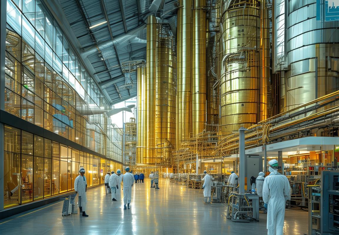
Environmental controlThe production of ICBs requires an environment that is free from contaminants. Factories use cleanroom facilities with air filtration systems that remove particles down to the nanoscale. These controlled environments are critical to prevent defects on the wafer’s surface and ensure the integrity of the circuits.
Continuous improvementThe technology in ICB production is constantly evolving. Factories invest heavily in research and development to improve existing processes and to develop new ones. This commitment to innovation ensures that ICBs continue to push the boundaries of what’s possible in electronics.
ConclusionThe state-of-the-art technology in ICB production is a marvel of human ingenuity. From the precision of photolithography to the automation of manufacturing processes, every aspect of ICB production is designed to produce the most efficient and reliable chips possible. As technology advances, so too does the capability of ICB factories, driving innovation and shaping the future of electronics.

The Impact of ICB Factories on Global Markets
In the intricate tapestry of global markets, the presence of integrated circuit board (ICB) factories stands as a pivotal force, shaping industries and economies alike. These factories, often unseen by the public eye, are the unsung heroes behind the scenes, crafting the very heart of modern technology. Let’s delve into the profound impact these factories have on the global stage.
The Power of ConnectivityICB factories are the architects of connectivity, providing the essential building blocks for the vast network of devices that keep the world connected. From smartphones to internet routers, the intricate circuitry produced in these factories ensures seamless communication across borders. This connectivity is not just a luxury but a necessity in today’s digital age, enabling businesses and individuals to operate and interact globally.
Driving Technological AdvancementThese factories are at the forefront of technological innovation. As they refine their processes and develop new techniques, they push the boundaries of what’s possible in electronics. The advancements in ICB production have led to the miniaturization of devices, improved energy efficiency, and enhanced performance. This continuous push for better technology not only benefits end-users but also spurs the development of new industries and applications.
Economic Engine of GrowthThe global presence of ICB factories has turned them into economic powerhouses. They create jobs, drive investment, and stimulate economic growth in the regions they operate. The ripple effect is significant, as these factories often support a vast ecosystem of suppliers, manufacturers, and service providers. The success of an ICB factory can have a domino effect, boosting local economies and contributing to national GDPs.
Supply Chain MasteryThe production of ICBs requires a sophisticated supply chain, with components sourced from all corners of the globe. ICB factories are not just manufacturing facilities; they are logistical hubs that manage complex networks of suppliers and distributors. This mastery over supply chain management is crucial for ensuring timely delivery and maintaining product quality, which are critical factors in a highly competitive global market.
Global Trade and RelationshipsICB factories are at the heart of global trade, acting as bridges between nations. They facilitate international trade agreements and partnerships, often becoming symbols of cooperation between countries. The reliance on these factories for critical components has fostered diplomatic relationships and economic alliances, making them instrumental in shaping global trade policies.
Market ResilienceThe impact of ICB factories on global markets extends to their role in market resilience. In times of economic downturn or geopolitical tension, these factories can adapt and continue operations, ensuring that the global supply of electronics remains stable. Their ability to pivot and innovate in the face of adversity is a testament to their importance in maintaining market stability.
Environmental ResponsibilityAs the world grapples with environmental challenges, ICB factories are increasingly focusing on sustainability. They are investing in green technologies, reducing waste, and minimizing their carbon footprint. This shift towards environmental responsibility is not just a moral imperative but also a strategic move, as consumers and governments demand more eco-friendly products and practices.
Intellectual Property and InnovationICB factories are hotbeds of intellectual property and innovation. They are at the forefront of developing new materials, manufacturing processes, and design techniques. The patents and proprietary knowledge generated within these factories are not only valuable assets but also drivers of future technological breakthroughs.
Consumer Expectations and ChoicesThe influence of ICB factories on global markets is also evident in the rise of consumer expectations. The demand for high-quality, efficient, and reliable electronics has been shaped by the capabilities of these factories. Consumers now expect seamless integration of technology into their daily lives, and ICB factories are the backbone of this expectation fulfillment.
In conclusion, the impact of ICB factories on global markets is multifaceted and profound. They are not just manufacturers but integral players in the global economic and technological landscape. Their role in connectivity, innovation, economic growth, and market stability cannot be overstated, making them a crucial component of the global ecosystem.
Challenges and Innovations in ICB Manufacturing
In the intricate world of integrated circuit board (ICB) manufacturing, challenges and innovations go hand in hand, shaping the landscape of technological progress. From precision requirements to environmental concerns, the industry faces a myriad of obstacles. However, through relentless innovation, manufacturers have developed groundbreaking solutions that push the boundaries of what’s possible.
The Push for PrecisionPrecision is paramount in ICB manufacturing, as even the smallest of errors can lead to malfunctioning circuits. Manufacturers grapple with the challenge of creating uniform layers of conductive materials, ensuring that every component fits perfectly within the designated space. Advanced lithography techniques, such as extreme-ultraviolet (EUV) lithography, have been developed to achieve sub-10nm resolutions, reducing the margin for error and enhancing the performance of ICs.
Environmental ConcernsThe semiconductor industry is not immune to environmental challenges. ICB factories generate a significant amount of hazardous waste and consume vast amounts of energy. Innovations in waste management and energy efficiency have become crucial. Recycling processes for chemical etchants and solvents, as well as the adoption of renewable energy sources, are becoming more prevalent. These advancements not only minimize the environmental impact but also reduce operational costs.
Material AdvancementsThe materials used in ICB manufacturing are continually evolving. Traditional silicon wafers are still the foundation, but researchers are exploring alternative materials like gallium nitride and silicon carbide, which offer higher thermal conductivity and can handle more power. These advancements pave the way for the development of more efficient and durable electronics.
Automation and RoboticsManual processes are being replaced by automation and robotics in ICB manufacturing. Automated assembly lines, such as those equipped with vision systems and robotic arms, can perform tasks with precision and consistency. This shift not only improves the quality of the final product but also increases production speed and reduces labor costs.
Heat Management InnovationsAs ICs become more complex and powerful, managing heat has become a significant challenge. Innovations in heat sinks, thermal vias, and phase-change materials help dissipate heat effectively. Additionally, the development of advanced packaging techniques, such as 3D ICs, allows for better thermal management and higher integration density.
Design for Manufacturing (DFM)DFM is a discipline that focuses on designing products that are easier and more cost-effective to manufacture. By considering the manufacturing process during the design phase, engineers can create ICs that are less prone to defects and require fewer resources. This approach has led to more efficient production and has become an integral part of the ICB manufacturing process.
Quality Control and ReliabilityMaintaining high-quality standards and ensuring product reliability are crucial in ICB manufacturing. Innovations in testing and verification processes, such as automated testing equipment and machine learning algorithms, help identify defects early in the production cycle. These advancements contribute to the longevity and dependability of electronic devices.
Supply Chain IntegrationThe complexity of the supply chain in ICB manufacturing requires continuous innovation. Manufacturers are working to integrate suppliers and partners more effectively, reducing lead times and improving the flow of materials. This integration also allows for better risk management and cost optimization.
Energy EfficiencyWith the growing awareness of climate change, energy efficiency has become a priority. Innovations in energy-saving technologies, such as LED lighting and energy-efficient HVAC systems, are being adopted in ICB factories. These measures not only reduce the carbon footprint but also contribute to a more sustainable manufacturing process.
Innovation in Process ControlThe precision required in ICB manufacturing demands advanced process control systems. Innovations in process control technology enable manufacturers to monitor and adjust production parameters in real-time, ensuring consistency and reducing the likelihood of errors. These systems are crucial for achieving the tight tolerances needed for modern ICs.
The integration of these challenges and innovations represents a continuous cycle of improvement in ICB manufacturing. As the industry evolves, so do the solutions, pushing the boundaries of what can be achieved in electronics. From material science to robotics, every aspect of ICB manufacturing is subject to constant innovation, driving technological advancements that impact industries worldwide.
The Future of ICB Factories
In the ever-evolving landscape of technology, integrated circuit board (ICB) factories stand as pivotal hubs of innovation and precision. As these factories push the boundaries of what’s possible, the future holds a myriad of possibilities, shaped by relentless advancements and the relentless pursuit of perfection.
The relentless demand for smaller, faster, and more efficient devices drives the need for more sophisticated ICB manufacturing processes. This relentless pursuit has led to the development of materials that defy the laws of physics, such as high-k dielectrics and metal gates, which enable transistors to switch faster and consume less power. The future of ICB factories is not just about producing smaller chips; it’s about producing chips that are more powerful and energy-efficient.
One of the most significant developments in ICB manufacturing is the rise of 3D stacking technology. This technique allows multiple layers of chips to be stacked on top of each other, significantly reducing the distance electrons must travel, thus improving performance and reducing power consumption. The future of ICB factories will see this technology becoming more prevalent, leading to the creation of systems-on-chips (SoCs) that are not just more powerful but also more compact.
The integration of AI and machine learning into the manufacturing process is another area poised for significant growth. AI algorithms can analyze vast amounts of data to optimize production lines, predict failures, and even suggest improvements in design. By using AI to monitor and adjust processes in real-time, ICB factories can achieve unprecedented levels of efficiency and quality control.
Material science is also playing a crucial role in shaping the future of ICB manufacturing. Graphene, a single layer of carbon atoms arranged in a hexagonal lattice, is being explored for its exceptional electrical conductivity and mechanical strength. If successfully implemented, graphene could lead to the development of faster and more durable ICs.
Energy efficiency is a key concern in the electronics industry, and the future of ICB factories will see a greater emphasis on creating chips that consume less power. This is not just about reducing costs; it’s about environmental responsibility. Innovations like the development of new semiconductor materials and processes that can handle higher levels of integration without compromising power consumption are at the forefront of research.
Another critical aspect of the future is the miniaturization of components. As devices get smaller, the need for microchips that can fit into increasingly tighter spaces grows. Advances in nanotechnology are making this possible, with the potential to shrink transistors to sizes that were once thought impossible. This miniaturization is not just for aesthetic reasons but is essential for the development of new devices that can fit into wearables, IoT devices, and other compact applications.
The complexity of ICBs is increasing at a rapid pace, and the future of manufacturing will require new tools and techniques to manage this complexity. Advanced lithography systems, which are used to pattern the tiny transistors on a chip, are becoming more complex, with some capable of printing features as small as 5 nanometers. These systems require a high degree of precision and control, and the development of new techniques to ensure accuracy will be crucial.
The environmental impact of ICB manufacturing is also a growing concern. The future of ICB factories will involve a shift towards more sustainable practices, including the recycling and reuse of materials and the reduction of harmful emissions. Innovations in energy production, such as the use of renewable energy sources, will play a significant role in making the ICB manufacturing process greener.
Lastly, the global nature of the electronics industry means that the future of ICB factories will be influenced by international trade agreements and geopolitical shifts. As countries compete for a share of the global market, the ability to produce cutting-edge ICs will become a strategic advantage. This competition will drive further innovation and investment in ICB manufacturing capabilities.
In conclusion, the future of ICB factories is a tapestry of technological advancements, from material science breakthroughs to the integration of AI and machine learning. It’s a future where smaller, faster, more efficient, and environmentally friendly chips will define the next generation of technology, and where ICB factories will be at the forefront of this transformation.
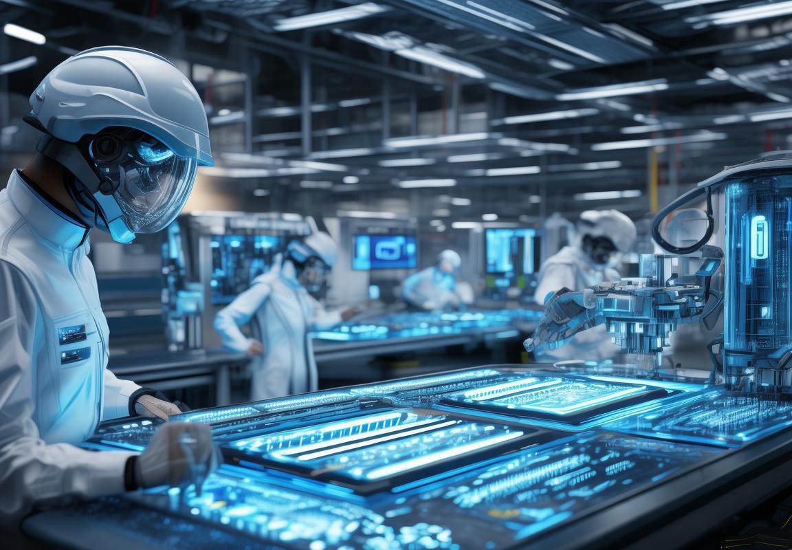
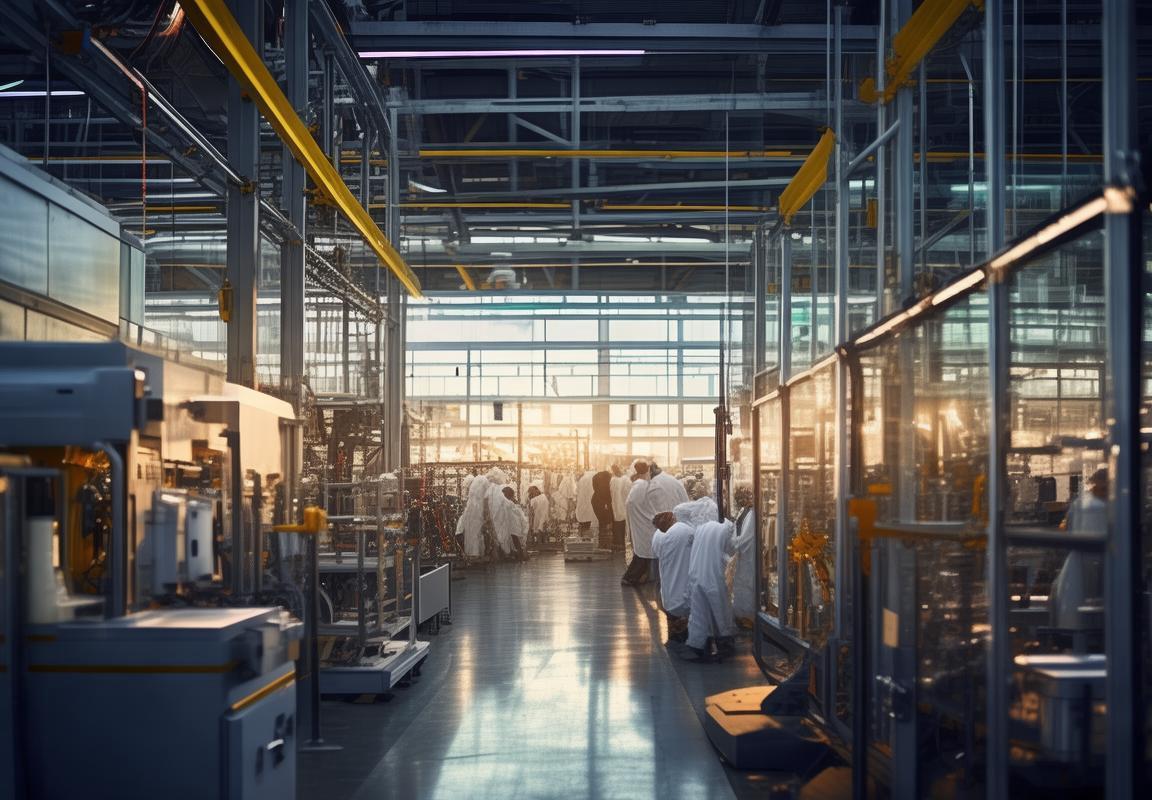
A Day in the Life at an ICB Factory
As dawn breaks over the industrial landscape, the hum of machinery begins to echo through the halls of an ICB factory. Workers file in, their days about to unfold in a symphony of precision and innovation. The factory, a sprawling complex of steel and glass, hums with the energy of progress. Here’s a glimpse into the day-to-day rhythm of life within these walls.
The morning rush is marked by the soft glow of screens as engineers review blueprints, ensuring that every component is designed to meet the exacting standards of modern electronics. The air is filled with the scent of soldering and the clink of tools as technicians prepare for the day’s tasks.
By 8 AM, the first shift is fully engaged. The assembly line, a marvel of engineering, starts to move. Workers in cleanroom attire, donned with protective suits and hairnets, glide between machines that hum with activity. Their eyes are focused, their hands steady as they place intricate chips onto the circuit boards.
Throughout the morning, the factory buzzes with activity. The precision of robots, designed for tasks like drilling and cutting, is matched by the deft hands of skilled laborers who handle delicate components with care. The process is a delicate balance of automation and human expertise.
As lunchtime approaches, the factory’s canteen comes alive. Workers gather, sharing stories of the morning’s achievements and challenges. The camaraderie is evident, a testament to the collective effort required to produce the intricate circuit boards that power our world.
After lunch, the pace picks up. Quality control inspectors move through the line, scrutinizing each board under magnifying glasses, ensuring that every connection is perfect. Defects are flagged, and the boards are sent back for rework, emphasizing the rigorous standards that govern the production process.
The afternoon brings a different kind of focus. Engineers analyze data from the day’s production, searching for trends and inefficiencies. They tweak algorithms and adjust machine settings to optimize performance and reduce waste.
As the day winds down, the factory begins to quiet. The line slows, and the last boards are processed. Workers gather to inspect their final product, a testament to their labor and the factory’s dedication to quality. The sense of pride is palpable as they watch the finished circuit boards being packaged and prepared for shipment.
In the late afternoon, the second shift is winding up. The night crew arrives, ready to take over. They review the day’s production, ensuring a smooth transition. The factory’s operations continue around the clock, with each shift playing a crucial role in the production cycle.
As night falls, the factory’s lights begin to dim, but the work goes on. The third shift takes over, their task to complete the day’s production run. The air is filled with the quiet whir of machines, the soft glow of screens, and the focused dedication of workers who know that their efforts contribute to the global supply chain.
The day comes to a close, and the factory, once a symphony of activity, now falls into a peaceful slumber. The workers head home, their spirits lifted by the knowledge that they have contributed to the marvels of modern technology. The ICB factory, a testament to human ingenuity and perseverance, continues to operate, its heart beating strong, ready to face another day of innovation and production.
The Environmental Footprint of ICB Factories
ICB factories, while instrumental in shaping the modern technological landscape, have a significant environmental footprint. This footprint encompasses various aspects, from the sourcing of raw materials to the disposal of waste. Here’s an in-depth look at the environmental challenges and considerations within these factories:
Materials and ExtractionThe production of integrated circuit boards begins with raw materials such as silicon, copper, and gold. The extraction of these materials often involves mining processes that can have devastating effects on ecosystems. Large-scale mining operations can lead to deforestation, soil erosion, and water contamination. The environmental impact is compounded by the energy-intensive processes required to refine these materials into usable forms.
Energy ConsumptionICB factories are massive energy consumers. The high temperatures needed for semiconductor manufacturing, combined with the constant operation of precision equipment, leads to substantial power usage. In many cases, this energy is sourced from fossil fuels, contributing to greenhouse gas emissions and climate change. Efforts to reduce this footprint include the adoption of renewable energy sources and the implementation of energy-efficient technologies.
Chemical Usage and WasteThe manufacturing of ICs involves the use of various chemicals, including etchants, solvents, and photoresists. These chemicals can be harmful to both human health and the environment if not managed properly. The disposal of chemical waste requires careful planning and adherence to environmental regulations. Factories often need to invest in advanced treatment facilities to neutralize and dispose of these chemicals safely.
Heat DissipationSemiconductor manufacturing generates a considerable amount of heat. This heat must be managed to prevent equipment damage and maintain the quality of the ICs. Traditional cooling methods, such as water chillers, can be energy-intensive. Innovations in heat dissipation, like phase-change materials and advanced heat sinks, are being explored to reduce energy consumption and lower the environmental impact.
Resource EfficiencyEfficiency in the use of resources is crucial in reducing the environmental footprint of ICB factories. This includes recycling and reusing materials, optimizing production processes to minimize waste, and improving the yield of each batch. Techniques like wafer-level packaging and 3D IC integration are not only technological advancements but also help in conserving materials.
E-Waste ManagementAs technology advances, older ICs and electronic devices are replaced, leading to a surge in electronic waste. Proper e-waste management is essential, as improper disposal can lead to hazardous materials leaching into soil and water. ICB factories are increasingly involved in recycling programs to reclaim valuable materials from discarded electronics, thus reducing the need for new resource extraction.
Regulatory ComplianceNavigating the complex web of environmental regulations is a constant challenge for ICB factories. Compliance with local, regional, and international laws can be difficult, especially when regulations vary significantly across different jurisdictions. Factories often need to invest in legal teams and environmental consultants to ensure they meet all requirements.
Sustainability InitiativesMany ICB factories are implementing sustainability initiatives to mitigate their environmental impact. These include the development of green buildings, the use of biodegradable materials, and the integration of sustainable practices into the supply chain. These efforts are not only environmentally responsible but can also enhance the company’s reputation and marketability.
Corporate Social Responsibility (CSR)ICB factories are increasingly embracing CSR as a core value. This involves more than just minimizing environmental impact; it includes promoting social well-being and economic development within the communities where the factories operate. CSR programs might include initiatives to educate local populations about environmental issues, support local businesses, or provide health care services.
Global Collaboration and StandardsAs the global market for ICs continues to grow, so does the need for collaboration and standardization in environmental practices. ICB factories are working with industry groups and regulatory bodies to develop global standards that can ensure a more sustainable approach to manufacturing without hindering technological progress.
In conclusion, the environmental footprint of ICB factories is a multifaceted issue that requires a comprehensive approach. From the sourcing of raw materials to the disposal of waste, every stage of the manufacturing process must be carefully managed. Innovations, collaborations, and a commitment to sustainability are crucial in reducing this footprint and ensuring a more eco-friendly future for the electronics industry.
The Role of ICB Factories in Future Tech Developments
In the ever-evolving landscape of technology, integrated circuit board (ICB) factories play a pivotal role in shaping the future. As the backbone of countless devices, from smartphones to autonomous vehicles, the advancements in ICB manufacturing are directly linked to groundbreaking technological developments. Let’s delve into the myriad ways ICB factories contribute to future tech.
The miniaturization of electronics is a testament to the prowess of ICB factories. With the ability to pack more transistors into smaller spaces, these factories enable the creation of devices that are not just compact but also powerful. This miniaturization has led to the development of wearables, IoT devices, and even medical implants, all of which rely on the intricate design and precision of ICBs.
ICB factories are at the forefront of quantum computing, a field that promises to revolutionize how we process information. As the foundation for quantum processors, ICBs are instrumental in creating the complex circuits needed for qubits to function. The development of quantum computers hinges on the ability of ICB factories to produce circuits with unparalleled precision and stability.
The rise of 5G technology has been a game-changer for connectivity, and ICB factories are crucial in this transformation. By manufacturing circuits capable of handling the high-speed data transfer and low latency required for 5G, these factories ensure that the next generation of smartphones, smart homes, and smart cities can operate seamlessly.
The automotive industry is undergoing a profound transformation with the advent of autonomous vehicles. ICB factories are integral to this shift, producing the sophisticated circuits needed for advanced driver-assistance systems (ADAS) and autonomous driving capabilities. These circuits enable the integration of complex sensors, processors, and communication modules that make autonomous driving possible.
In the realm of healthcare, ICB factories are contributing to life-saving innovations. The miniaturization of medical devices, such as implantable defibrillators and glucose monitors, has been made possible by the precision and miniaturization of ICBs. These advancements not only improve patient outcomes but also enhance the quality of life.
The Internet of Things (IoT) is a network of interconnected devices that communicate and share data. ICB factories are the driving force behind the development of these devices, from smart thermostats to industrial sensors. The ability to produce circuits with a wide range of functionalities and power efficiency is crucial for the widespread adoption of IoT technology.
The rise of AI and machine learning is another area where ICB factories are making significant strides. As the engines of AI systems, processors with complex ICBs are essential for handling the massive data processing required for AI algorithms. The ability to produce these processors at scale and with high performance is vital for the advancement of AI technology.
The development of advanced materials for ICBs is another critical aspect of future tech. Graphene, for instance, offers exceptional conductivity and flexibility, which could lead to the creation of next-generation circuits that are not only faster but also more durable. ICB factories are at the forefront of integrating these materials into their manufacturing processes.
The integration of sensors into ICBs is also a key development. Sensors are becoming an integral part of everyday devices, from fitness trackers to smart agriculture systems. The ability to produce multi-functional circuits with embedded sensors is opening up new possibilities across various industries.
As the demand for energy-efficient electronics grows, ICB factories are innovating to produce circuits that consume less power. This is particularly important for battery-powered devices, as it extends battery life and reduces the environmental impact.
In conclusion, the role of ICB factories in future tech developments is undeniable. From enabling the miniaturization of electronics to driving advancements in quantum computing, 5G, and autonomous vehicles, these factories are the silent architects of the future. Their continuous innovation and adaptation to new technologies will be the key to unlocking the next wave of technological breakthroughs.